


Cleaning Process in FAB
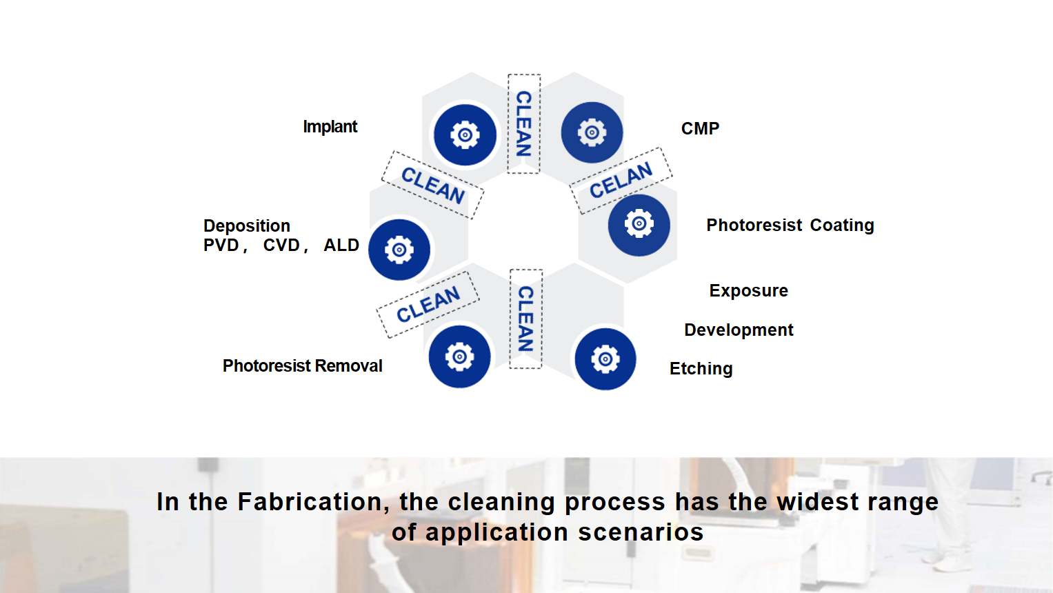
Wafer cleaning is a crucial step in the semiconductor manufacturing process. It not only directly affects the quality and yield of the chip, but also closely related to the reliability of the final product. The main purpose of wafer cleaning is to remove various contaminants generated during the manufacturing process, such as particles, chemical residues, oxide layers, and organic impurities. Each manufacturing process generates different types of contaminants, and the type and method of cleaning must be selected according to the specific process needs.
During the wafer preparation phase, surface contaminants and oxides need to be removed. The lithography stage is central to semiconductor manufacturing, where the surface of the wafer is coated with photoresist and then exposed and developed to form a circuit pattern at the micron level. After the development process, residues of the photoresist may adhere to the wafer surface. If these residues are not completely removed, they will have a negative impact on subsequent processes such as etching and deposition, and even affect the functionality of the chip. The second is during the etching process, where tiny chemicals or etching by-products often adhere to the wafer surface after etching. If these substances are not removed, they can affect the subsequent process and may even form an uneven film on the surface of the wafer, leading to defects or device failure. Subsequent thin film deposition, etc., are processes that need to be cleaned.
Wafer cleaning is an integral part of the semiconductor manufacturing process and involves multiple steps. From the removal of oxides, contaminants, and photoresist residues from the wafer surface, to the removal of by-products after etching, to ensuring the cleanliness of the metal interconnect, every step of the cleaning process is designed to ensure the performance and reliability of the final chip. The choice of cleaning process depends not only on the nature of the contaminant, but also on the manufacturing process, the condition of the equipment, and the technical requirements of the final product. Our company's scientists and engineers are aware of our customers' production needs. We offer a broad portfolio of market-leading products for etching, photoresist stripping, and wafer cleaning, among others, which are complementary processing steps throughout the semiconductor manufacturing process.

Address: 101 & 201, East Unit; 102 & 202, West Unit, Building 8, Phase I, Block V, Hengtai IMP, Suzhou Nano City, No. 75 Pudian Road, Suzhou Industrial Park
Public account